(China (Mainland))

Product Summary
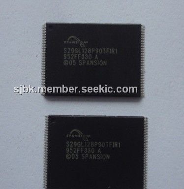
The S29GL128P90TFIR10 is a 3.0 Volt-only page mode flash memory featuring 90 nm mirrorbit process technology. The device offers a fast page access time of 25 ns with a corresponding random access time as fast as 90 ns. It features a Write Buffer that allows a maximum of 32 words/64 bytes to be programmed in one operation, resulting in faster effective programming time than standard programming algorithms. This makes the S29GL128P90TFIR10 ideal for today’s embedded applications that requires higher density, better performance and lower power consumption.
Parametrics
S29GL128P90TFIR10 absolute maximum ratings: (1)Storage Temperature, Plastic Packages: -65℃to +150℃; (2)Ambient Temperature with Power Applied: -65℃ to +125℃; (3)Voltage with Respect to Ground, All Inputs and I/Os except as noted below: -0.5 V to VCC + 0.5 V; VCC: -0.5 V to +4.0 V; VIO: -0.5V to +4.0V; A9 and ACC: -0.5 V to +12.5 V; (4)Output Short Circuit Current: 200 mA
Features
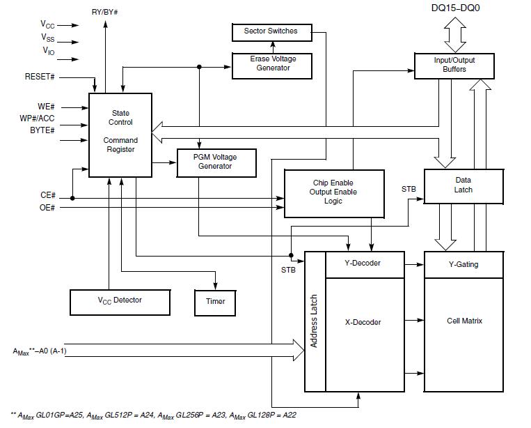
S29GL128P90TFIR10 features: (1)Single 3V read/program/erase (2.7-3.6 V); (2)Enhanced VersatileI/O. control, All input levels (address, control, and DQ input levels) and outputs are determined by voltage on VIO input. VIO range is 1.65 to VCC; (3)90 nm MirrorBit process technology; (4)8-word/16-byte page read buffer; (5)32-word/64-byte write buffer reduces overall programming time for multiple-word updates; (6)Secured Silicon Sector region: 128-word/256-byte sector for permanent, secure identification through an 8-word/16-byte random Electronic Serial Number; Can be programmed and locked at the factory or by the customer; (7)Uniform 64Kword/128KByte Sector Architecture: One hundred twenty-eight sectors; (8)100,000 erase cycles per sector typical; (9)20-year data retention typical; (10)Offered Packages: 56-pin TSOP; 64-ball Fortified BGA; (11)Suspend and Resume commands for Program and Erase operations; (12)Write operation status bits indicate program and erase operation completion; (13)Unlock Bypass Program command to reduce programming time; (14)Support for CFI (Common Flash Interface); (15)Persistent and Password methods of Advanced Sector Protection; (16)WP#/ACC input: Accelerates programming time (when VHH is applied) for greater throughput during system production; Protects first or last sector regardless of sector protection settings; (17)Hardware reset input (RESET#) resets device; (18)Ready/Busy# output (RY/BY#) detects program or erase cycle completion.
Diagrams
| Image | Part No | Mfg | Description |  |
Pricing (USD) |
Quantity | ||||||||||||
|---|---|---|---|---|---|---|---|---|---|---|---|---|---|---|---|---|---|---|
 |
 S29GL128P90TFIR10 |
Spansion |
Flash 3V 128Mb Mirrorbit highest address 90ns |
Data Sheet |
|
|
||||||||||||
| Image | Part No | Mfg | Description | |
Pricing (USD) |
Quantity | ||||||||||||
 |
S29GL016A |
Other |
|
Data Sheet |
Negotiable |
|
||||||||||||
|
S29GL01GP |
Other |
|
Data Sheet |
Negotiable |
|
||||||||||||
|
S29GL01GP11FAIR10 |
Spansion |
Flash IC 1GIG 3.0V FLSHMEM |
Data Sheet |
|
|
||||||||||||
|
S29GL01GP11FAIR20 |
Spansion |
Flash 1GB 3.0-3.6V 110ns |
Data Sheet |
|
|
||||||||||||
|
S29GL01GP11FFCR10 |
Spansion |
Flash 1GB 3.0-3.6V 110ns PBF |
Data Sheet |
|
|
||||||||||||
|
S29GL01GP11FFCR20 |
Spansion |
Flash 1GB 3.0-3.6V 110ns PBF |
Data Sheet |
|
|
||||||||||||